Follow
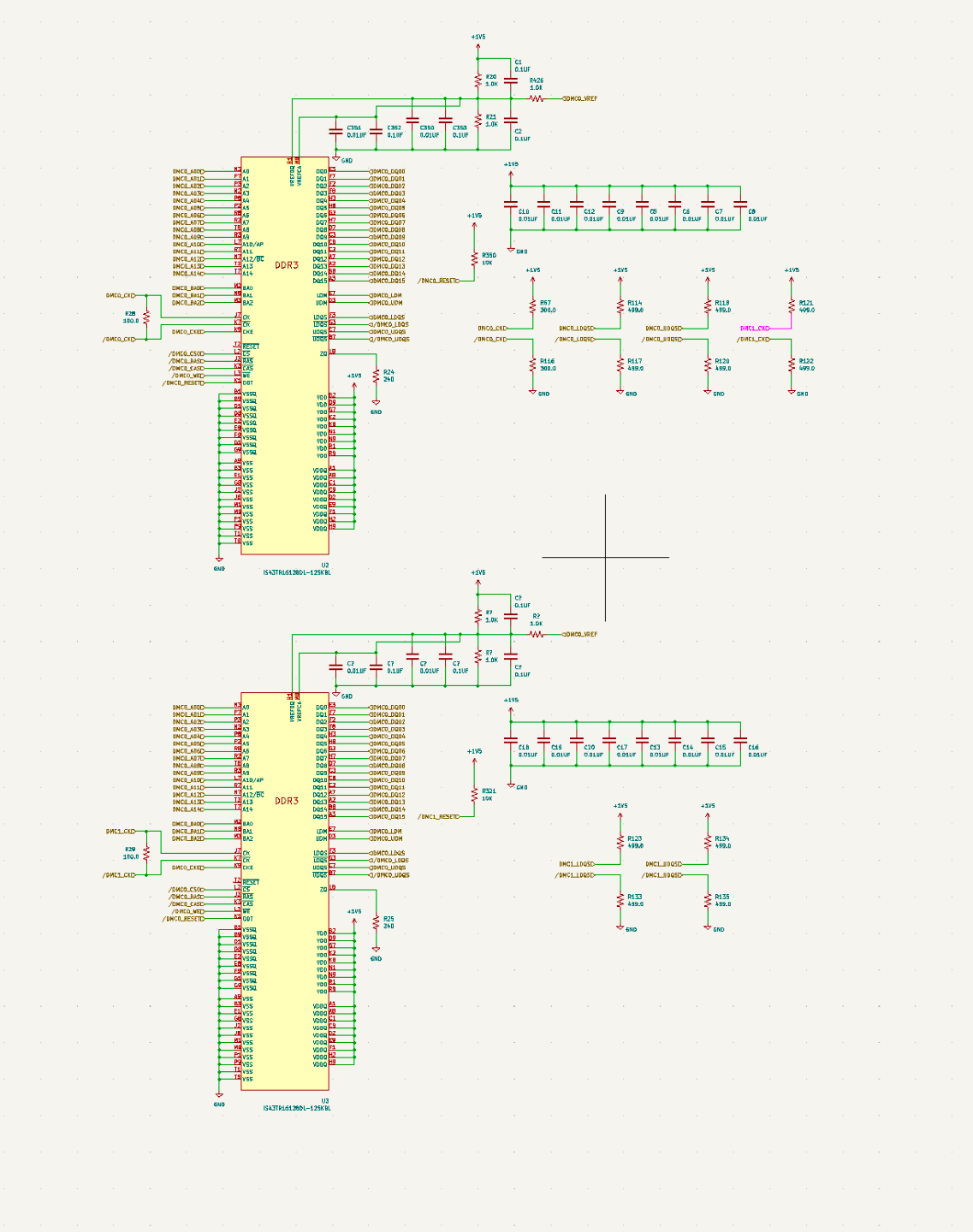
ADSP 589 mini reference design: Memory interface - one of the trickiest parts of this design. I've run through most of the pinouts, outside of labelling some pins on the second memory chip. The first schematic page (of 8) is almost complete.